Getting to know Vivado
Design with Block Design
Release date: Feb 22, 2023
In the previous article, we created a function to blink a single LED using VerilogHDL. Vivado also allows you to visually arrange your designed modules in block units and design them as a Block Diagram. This feature is called Block Design. This article uses Block Design to modify the design to place two Blink modules and blink two LEDs. We will change the Project in the previous article.
Table of Contents
Add Blink module to Block Design
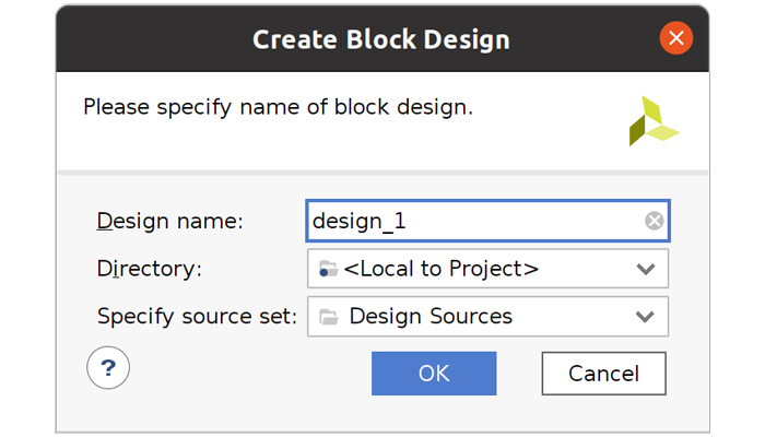
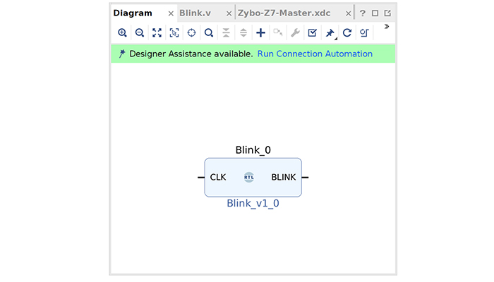
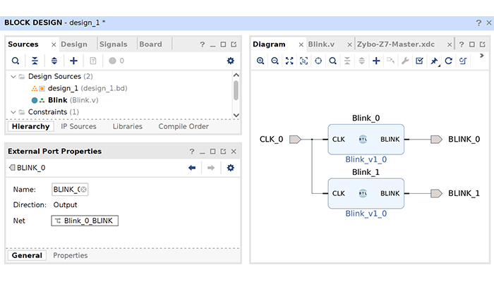
From IP INTEGRATOR in Flow Navigator, run Create Block Design. Design name is assumed to be OK with the default value.
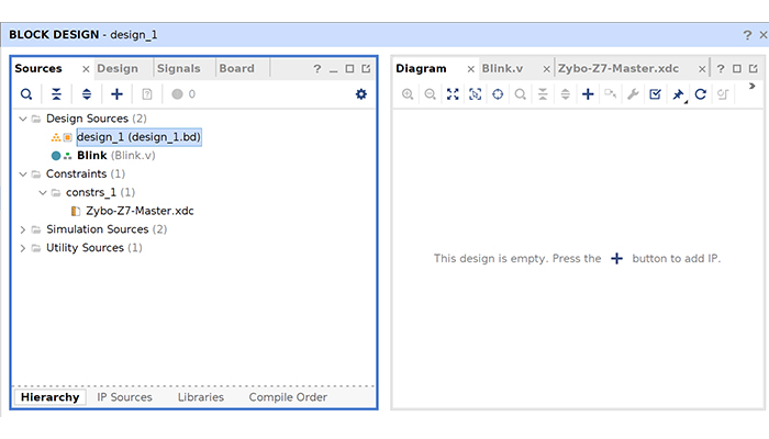
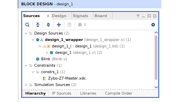
design_1(design_1.bd) will be added to Design Sources.
Add the Blink module to Block Design.
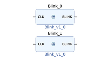
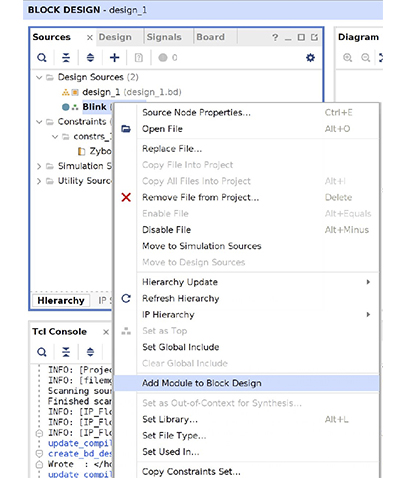
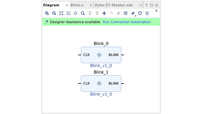
Right-click on Blink in Design Sources and execute Add Module to Block Design. Blink_0 will be added to Diagram. Repeat the same operation to add another Blink module. To distinguish it from the first module added, it is added under the name Blink_1.
Signal connection
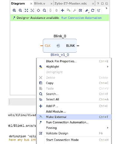
Connect signals for the added modules.
CLK is input externally to Block Design. The BLINK signal is also output outside of Block Design. This condition is expressed in Diagram.
Click and highlight the CLK pin of Blink_0 in the diagram, then right-click and execute Make External. A Port named CLK_0 is added as an input. Since the same CLOCK is to be input to Blink 1, connect the CLK pin of Blink_1 to CLK_0.
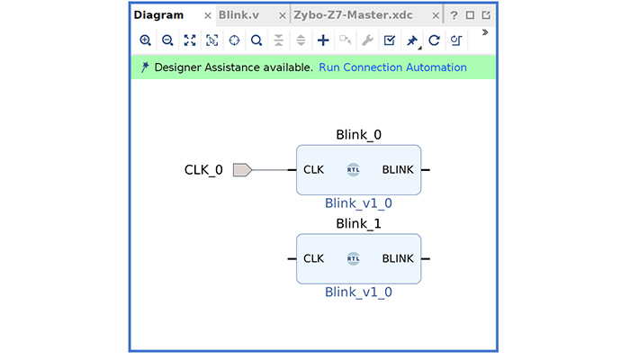
Also, for BLINK, each Make External is executed separately to make it an output Port. The properties of the added Port can be viewed at External Port Property. The Port Name is assigned automatically, but can also be changed from Property.
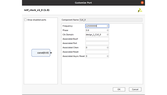
Although there is no particular impact on this topic, write the correct frequency in the CLK_0 frequency.
Since Zybo is designed with a 125 MHz clock, double-click the CLK_0 port in the Block Design and set the frequency from the Customized port.
Block Design is now complete.
Create HDL Wrapper
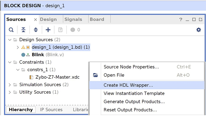
Creating a Block Design alone does not complete the design.
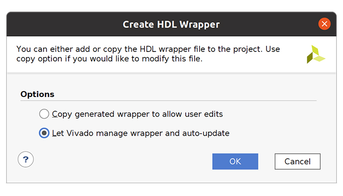
The Create HDL Wrapper must be run. This operation inserts an HDL file that serves as the Top module on top of Block Design. Right click on design_1 (design_1.bd ) in Design Sources and run Create HDL Wrapper. A dialog box will be displayed, but the default values are OK.
design_1_1_wrapper (design_1_wrapper.v ) is created in Design Sources.
Change the constraint file
Check the design_1_wrapper.v that you just created. The design_1_wrapper is described as the top module, and BLINK_0, BLINK_1, and CLK_0 are defined for input and output. These signals must be connected to the desired terminals.
module design_1_wrapper
  (BLINK_0,
   BLINK_1,
   CLK_0);
 output BLINK_0;
 output BLINK_1;
 input CLK_0;

 wire BLINK_0;
 wire BLINK_1;
 wire CLK_0;

 design_1 design_1_i
      (.BLINK_0(BLINK_0),
       .BLINK_1(BLINK_1),
       .CLK_0(CLK_0));
endmodule
This time, the connection is made as follows
##Clock signal
set_property -dict { PACKAGE_PIN K17   IOSTANDARD LVCMOS33 } [get_ports { CLK_0 }]; #IO_L12P_T1_MRCC_35 Sch=sysclk
create_clock -add -name sys_clk_pin -period 8.00 -waveform {0 4} [get_ports { CLK_0 }];

##LEDs
set_property -dict { PACKAGE_PIN M14   IOSTANDARD LVCMOS33 } [get_ports { BLINK_0 }]; #IO_L23P_T3_35 Sch=led[0]
set_property -dict { PACKAGE_PIN M15   IOSTANDARD LVCMOS33 } [get_ports { BLINK_1 }]; #IO_L23N_T3_35 Sch=led[1]
operation check
As in the previous step, run Generate bitstream and check its operation. LD0 and LD1 blink at the same timing.
*All names, company names, product names, etc. mentioned herein are trademarks or registered trademarks of their respective companies.