Getting to know Vivado
Try blinking LEDs with Programable Logic
Release date: January 5, 2023
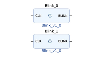
Design a Logic to blink LEDs in Verilog HDL. Readers will understand the sequence of steps from coding to operation check. The Logic to be designed is a simple module that divides an incoming clock and outputs it.
Table Of Contents
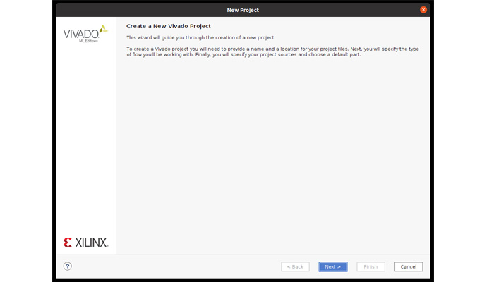
Create A Project
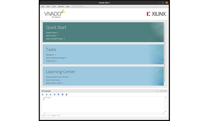
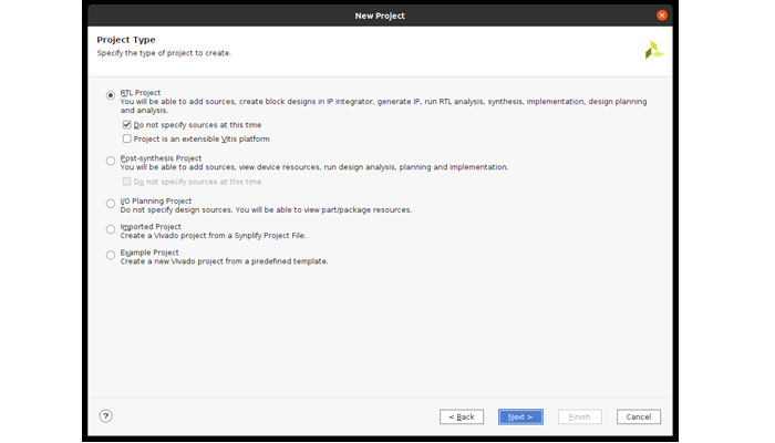
Start Vivado and create a new project from CreateProject>.
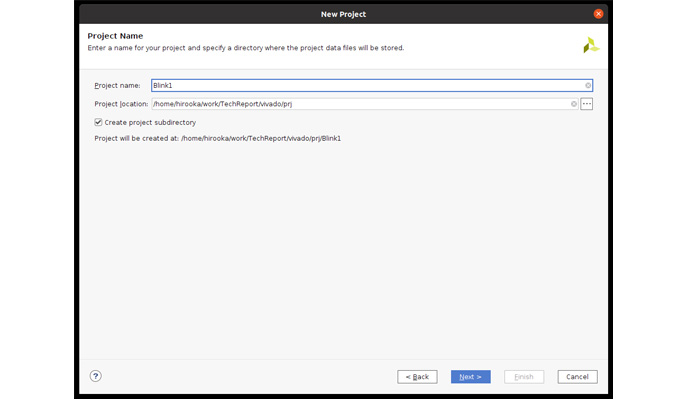
The project name isBlink1.
For Project Type, select RTL Project and clickDo not specify sources at this time checkbox. It means that the source code will not be specified when the project is created. After the project is created, the source code will be written.
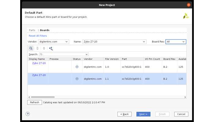
Select the target board. There are several versions of Zybo Z7-20, so please select the Board file of the version that matches the Zybo Z7 you have purchased.
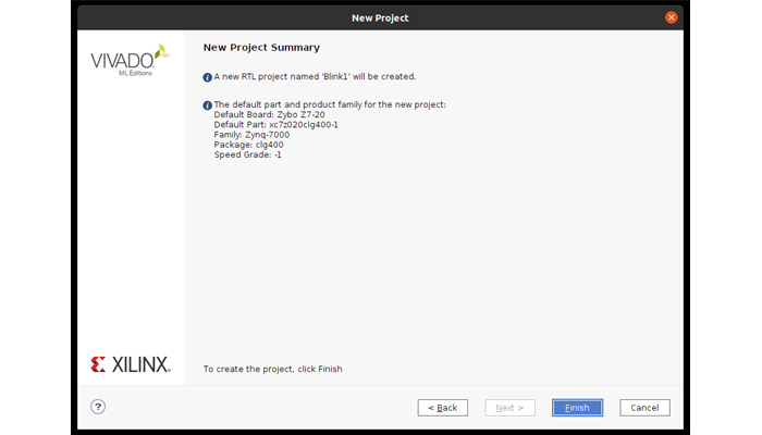
By reading the Board file, information dependent on the hardware design (PCBA design) is read into Vivado. This completes the project creation. A summary will be displayed, so please check for any errors in key items such as the device to be designed.
Create Source Code
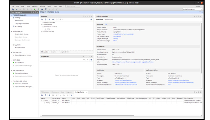
Operations related to the Project are performed from the Flow Navigator.
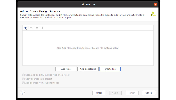
Add Sources in PROJECT MANAGER in Flow Navigater. The source code will be created when you select Add or create design sources.

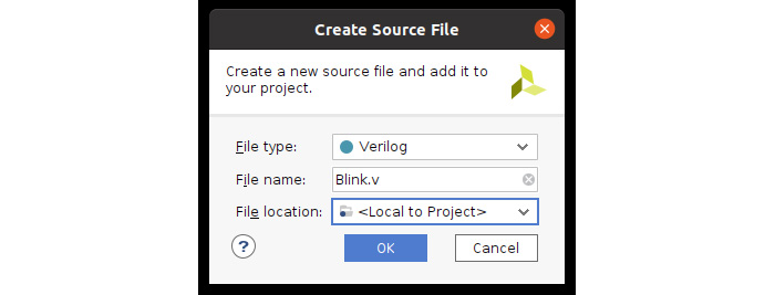
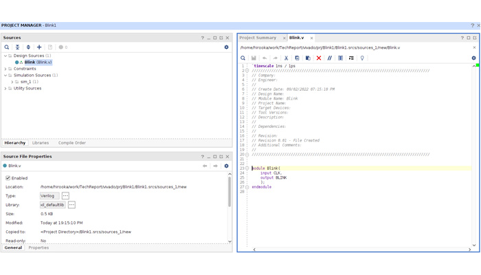
We create a new source file. Click Create File to create Blink.v. Then enter the information to generate a prototype of the module to be designed.
If this flow is too cumbersome, you can create the source code in advance, and then use the Add File. The source code is written in Verilog HDL.
This time, we will follow the guidance of TOOL and write the source code.
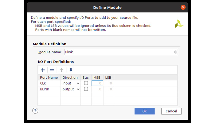
Add the following module name: Blink, and add 1 bit each of input and output signals as follows.
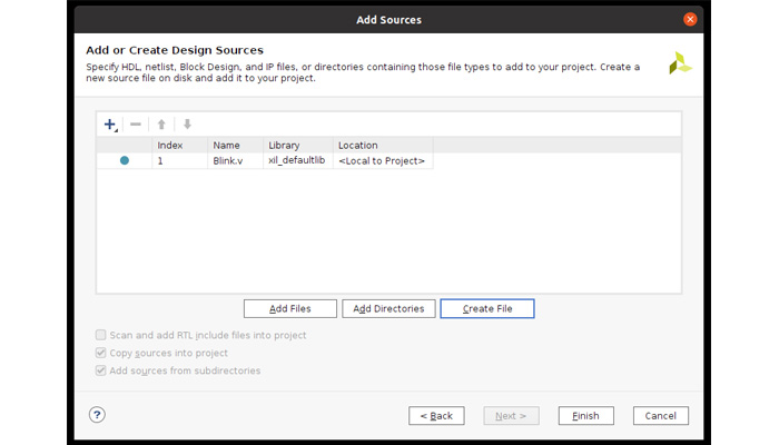
Blink is added to the Source pane.
Added Blink.v, the data will be stored in the Blink1/Blink1.srcs/sources_1/new.
Add the necessary source code.
module Blink(
input CLK, // 125MHz
output reg BLINK =0
);

parameter C_Blink_Time = 32'h01000000;// 2^24 * 125MHz = 0.134sec

reg[31:0] rCnt =0;

always @(posedge CLK) begin

	if( rCnt == C_Blink_Time ) begin
		BLINK <= !BLINK;
		rCnt <= 0;
	end

	else begin
			rCnt <= rCnt + 1;
	end

end
endmodule
Add a Constraints File
As described in the source code, the LED blinks by counting the input clock and turning the signal HIGH ⇔ LOW at regular time intervals.
Here, the Which LEDs do you flash?" question arises. This question can be resolved by adding a constraints file. In the constraints file, timing constraints and physical constraints can be described. The constraints file description serves as a link between the FPGA internal logic design and the board (PCBA) design using the FPGA. Therefore, the description must take the PCBA design into account.
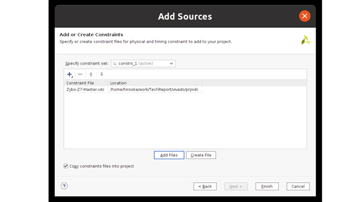
We will not discuss the constraints file further here. For Zybo Z7, Digilent has released a master constraints file, which we will modify and use in this design.
Add a constraints file
From Add Sources in PROJECT MANAGER in Flow Navigator, select Add or create a constraints and add Zybo-Z7-Master.xdc.

Edit a Constraints File
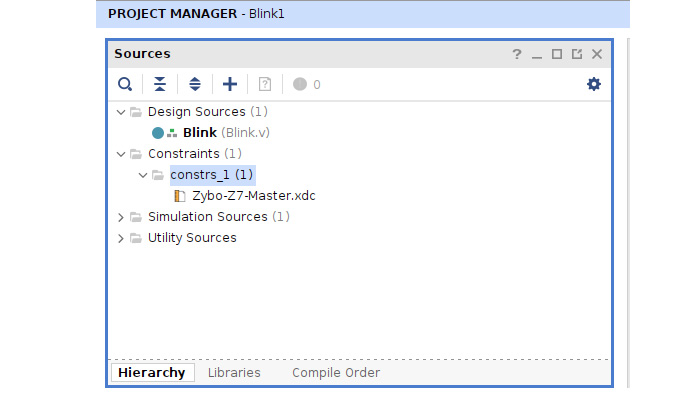
A constraints file has been added to the Source pane, so open it in Vivado's editor and edit it.
Write the file in order for LED0 to blink. In order to control the blinking time, activate the clock signal to count. The Clock is the sysclk signal that is input to Pin K17 from the Clock output pin of the Ethernet PHY IC. This is described in lines 8~9 of the added constraints file. To make it valid, uncomment it. The # at the beginning of the line is a comment. The signal name defined in the Blink module is described as CLK, so replace sysclk with CLK. Now we have assigned the signal on Pin K17 to the CLK of the designed logic.
set_property -dict { PACKAGE_PIN K17   IOSTANDARD LVCMOS33 } [get_ports { CLK }]; #IO_L12P_T1_MRCC_35 Sch=sysclk
create_clock -add -name sys_clk_pin -period 8.00 -waveform {0 4} [get_ports { CLK }];
Next, the output signal BLINK is assigned to LED0, which is connected to M14 Pin in the board design.
Uncomment line 27 and replace LED[0] with BLINK.
set_property -dict { PACKAGE_PIN M14 IOSTANDARD LVCMOS33 } [get_ports { BLINK }]; #IO_L23P_T3_35 Sch=led[0]The source code is now ready.
Create Bit Stream
From the source code written in HDL and the constraints file, a BitStream file is created to generate the circuit on FPGA. After RTL development, the process to generate the BitStream is divided into several stages. For an overview of the flow, see Vivado Design Suite User Guide: Design Flow Overview (UG892).
| Stage | |
|---|---|
| SIMULATION | Simulation of circuits described in HDL is performed. *Skip Here. |
| RTL ANALYSIS | Analyze and verify designs at each stage of logic synthesis, place and route, etc. We will not mention it here. |
| SYNTHESIS (Logic Synthesis) |
Converts HDL source code to circuit level and outputs a netlist. This process does not yet take into account physical terminal locations or timing constraints. |
| IMPLEMENTATION (Placement And Wiring) |
Optimize and place and route from the synthesized netlist to the device resources available on the target device. Circuit-level logic is mapped to the actual device so that logic can be configured inside the FPGA. Place and route is performed to satisfy the physical and timing constraints described in the constraints file. |
While the flow is described above, the actual procedure is very easy to follow. Synthesis, Run Implementation, and Generate Bitstream are automatically executed in sequence.
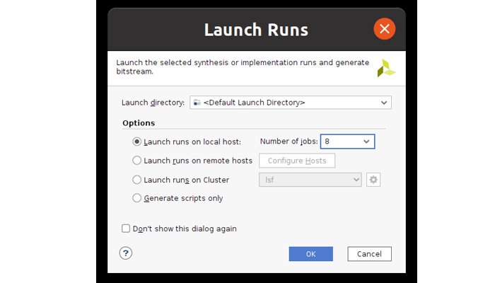
When you have completed up to BitStream Generation, the following dialog box will appear. This time, cancel it.
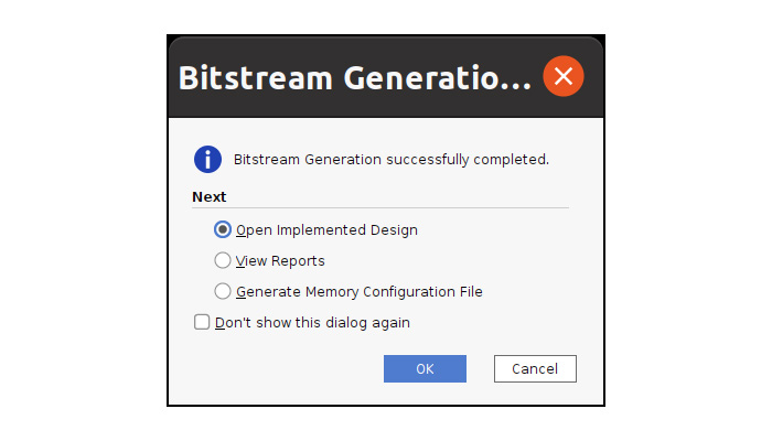
A BitStream file with the file name Blink.bit is generated below Blink1/Blink1.runs/impl_1.
Operation Check
Write the generated BitStream file to the actual device to check its operation.
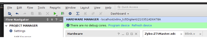
Use Vivado to write BitStream files. Connect the microUSB terminal (J12) of Zybo-Z7 to the PC with a USB cable and turn on the power switch of Zybo-Z7. From PROGRAM AND DEBUG in Flow Navigator, execute Open Hardware Manager -> Open Target -> Auto Connect. If the hardware is successfully connected, the HARDWARE MANAGER will start as shown below.
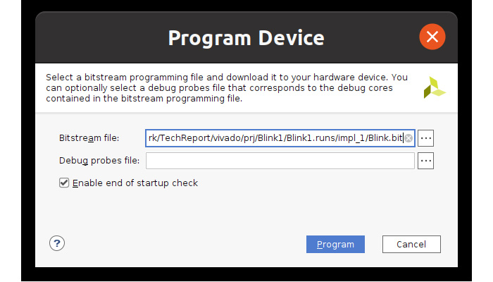
Now download the BitStream file from the Program device. Then, select Blink.bit and click on the Program Button.
When the download is complete, LED0 starts blinking.
Resources
| File-Name | Remarks | Download |
|---|---|---|
| Blink.v | Verilog Source Code describing the Blink module | Download |
| Zybo-Z7-Master.xdc | Constraints file for operation check | Download |
*All names, company names, product names, etc. mentioned herein are trademarks or registered trademarks of their respective companies.